Atlas Global Equity Income – Monthly Manager Commentary
April 2026

During April we initiated new positions in Lam Research & NVIDIA. Lam Research supplies critical etching and deposition equipment to semiconductor manufacturers. NVIDIA is a dominant provider of semiconductors predominantly Graphic Processing Units (GPU) used in data centres. We sold positions in LVMH and Ryanair to fund the purchases.
Featured holding – SK Hynix
The computer memory industry was once characterised by fierce competition and volatile prices. Today, after decades of low profits and consolidation, it is a stable oligopoly dominated by three major players: SK Hynix, Samsung and Micron.
Thanks to artificial intelligence (AI), computer memory – particularly High Bandwidth Memory (HBM) – is now in high demand. The market structure of the industry, the huge capital expenditure required to build memory fabrication plants and the complexities of manufacturing HBM are allowing the oligopoly to capture more of the value chain than the industry did previously.
Memory prices have risen dramatically, and Micron recently announced a memory five-year contract – something almost unheard of in the industry. Press reports suggest SK Hynix and Samsung are seeking to secure similarly lengthy deals. SK Hynix, the clear leader in current-generation HBM3E, is well placed to benefit as the industry transitions to HBM4.
Memory basics
There are two main types of memory:
- DRAM (dynamic random-access memory) is the high-speed, volatile memory that serves as a computer’s main working memory, holding data and programs while the device is powered on. “Volatile memory” simply means the memory is lost when the power to the computer is switched off. HBM is an advanced type of DRAM.
- NAND flash is a non-volatile memory used for long-term storage in solid-state drives, USB sticks and smartphones. It retains data even when power is off.
We are going to focus on the DRAM market in this article. First, though, it is worth taking a look at some history and how the market structure of the industry has evolved.
History of the memory market
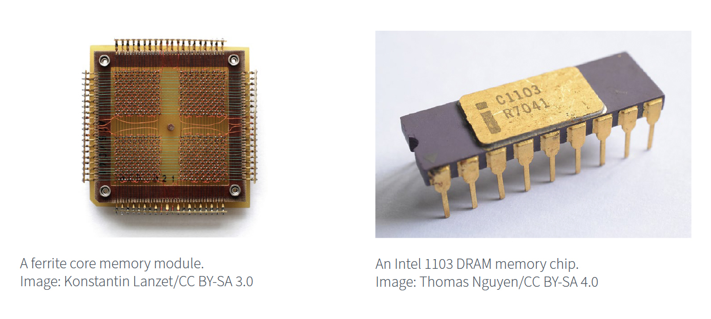
The dominant memory technology before silicon was magnetic core, which employed a grid of tiny ferrite rings to store bits of data using magnetic fields. This technology was widely used in computers from the mid-1950s until the early 1970s, but it was bulky and difficult to shrink in size.
Intel introduced the 1103, the world’s first commercially successful 1-kilobit DRAM chip, in 1970. It was a breakthrough because it offered dramatically lower cost, smaller size and higher density than magnetic core memory, making semiconductor memory practical.
To put this in perspective: the 1103 could store 1,024 bits – which, at 8 bits per character, could store only 128 characters. This is barely enough memory to retain the previous sentence! Nonetheless, it was revolutionary and marked the start of the silicon memory industry.
The success of the 1103 led to a wave of competition.
A number of smaller firms – including Mostek, Advanced Memory Systems (AMS) and Unisem – entered the market. Texas Instruments became a significant competitor in 1973, with its 4k DRAM chip, followed by other US companies, including National Semiconductor, Motorola, Fairchild Semiconductor and Intersil.
The next wave of competition came from Japanese firms, with NEC, Hitachi, Fujitsu, Toshiba and Mitsubishi quickly ramping up production. Benefiting from manufacturing scale, quality and pricing, these companies made ever-greater inroads during the late 1970s and early 1980s and eventually gained an 80% share of the global market.
By 1985 the Japanese producers’ aggressive low-cost production had triggered severe price crashes, forcing Intel, Mostek, Fairchild Semiconductor, National Semiconductor, Motorola and most other US companies to exit the industry. They just could not stomach the financial losses. (As it happened, Intel’s decision to exit the memory business and focus on microprocessors proved to be one of its best-ever corporate strategies.)
Yet the world still had an insatiable appetite for memory chips, and relentless global demand soon attracted South Korean conglomerates. In the mid-1980s, backed by strong government industrial policy and patient capital, Samsung Electronics and Hyundai Electronics (later SK Hynix) entered the DRAM market. South Korea was determined to shift its economy away from low-wage assembly industries and textile manufacturing towards high-tech, higher-value industries. Samsung licensed its initial 64k DRAM technology from Micron – one of the few major US companies that had resolved to stay the course.
There were many victims in the years that followed. In 1998, for example, to escape brutal price volatility and focus on the more profitable analog chip market, Texas Instruments sold its DRAM operations to Micron. By the early 2010s, in the face of South Korea’s rise, most Japanese companies had exited, with the final major player, Elpida Memory – formed from a merger of NEC,Hitachi and Mitsubishi operations – filing for bankruptcy in 2012.
For decades, too much capital had chased the promise of financial rewards from computer memory. Waves of over-supply and volatile prices had crushed that dream. DRAM had become the archetypal commodity product.
Amid the fallout, in 2001, the Hyundai Group sought to distance itself from the deeply unprofitable memory business. Still burdened by massive debt after the 1997 Asian financial crisis, it span out SK Hynix.
Fast-forward to the present day and we find SK Hynix, Samsung and Micron controlling over 90% of DRAM manufacturing. Remaining in the industry has been a long, hard slog that has brought questionable rewards for these three survivors.
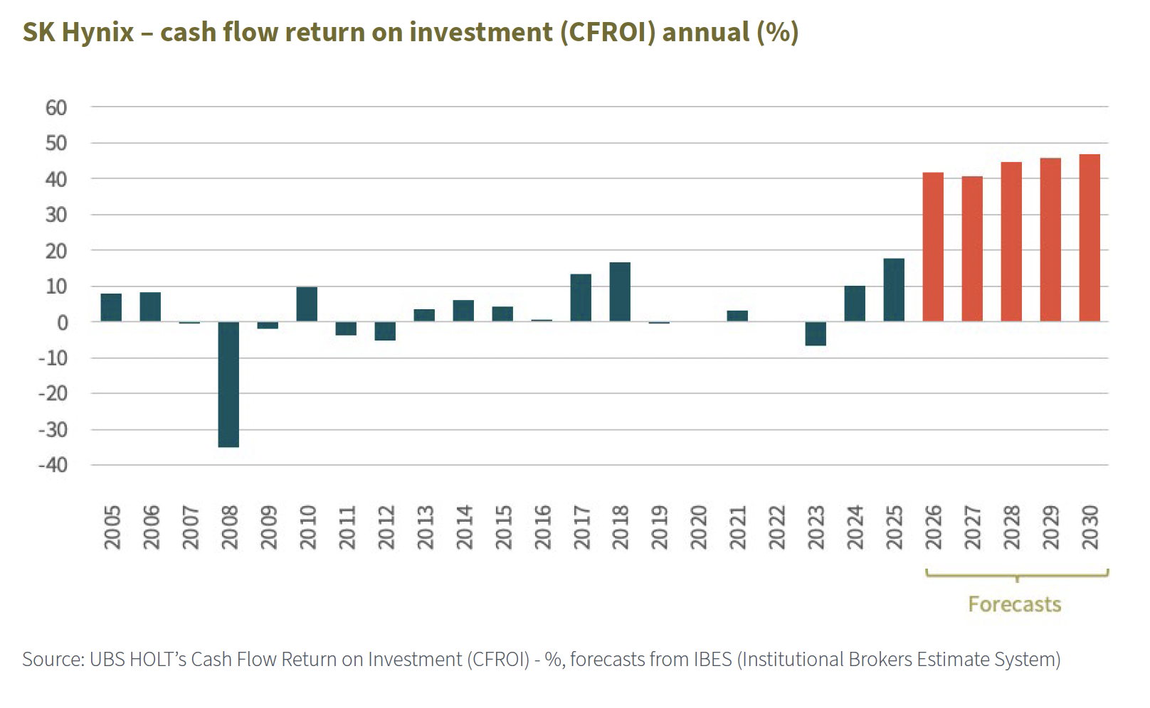
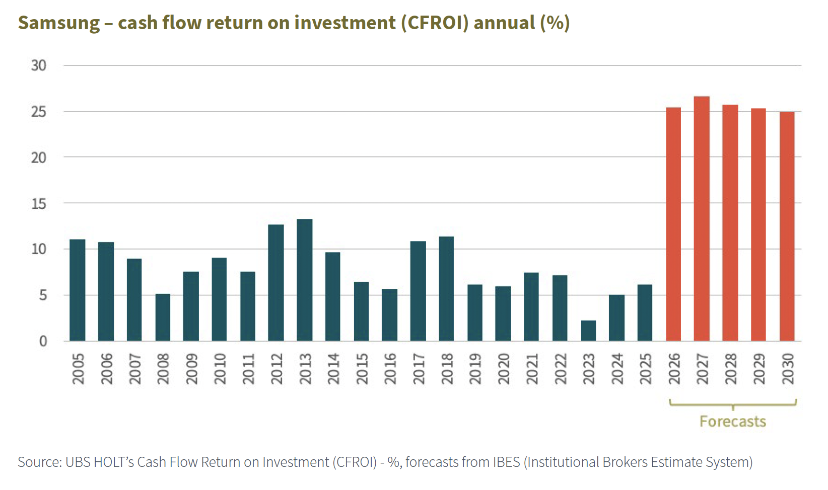
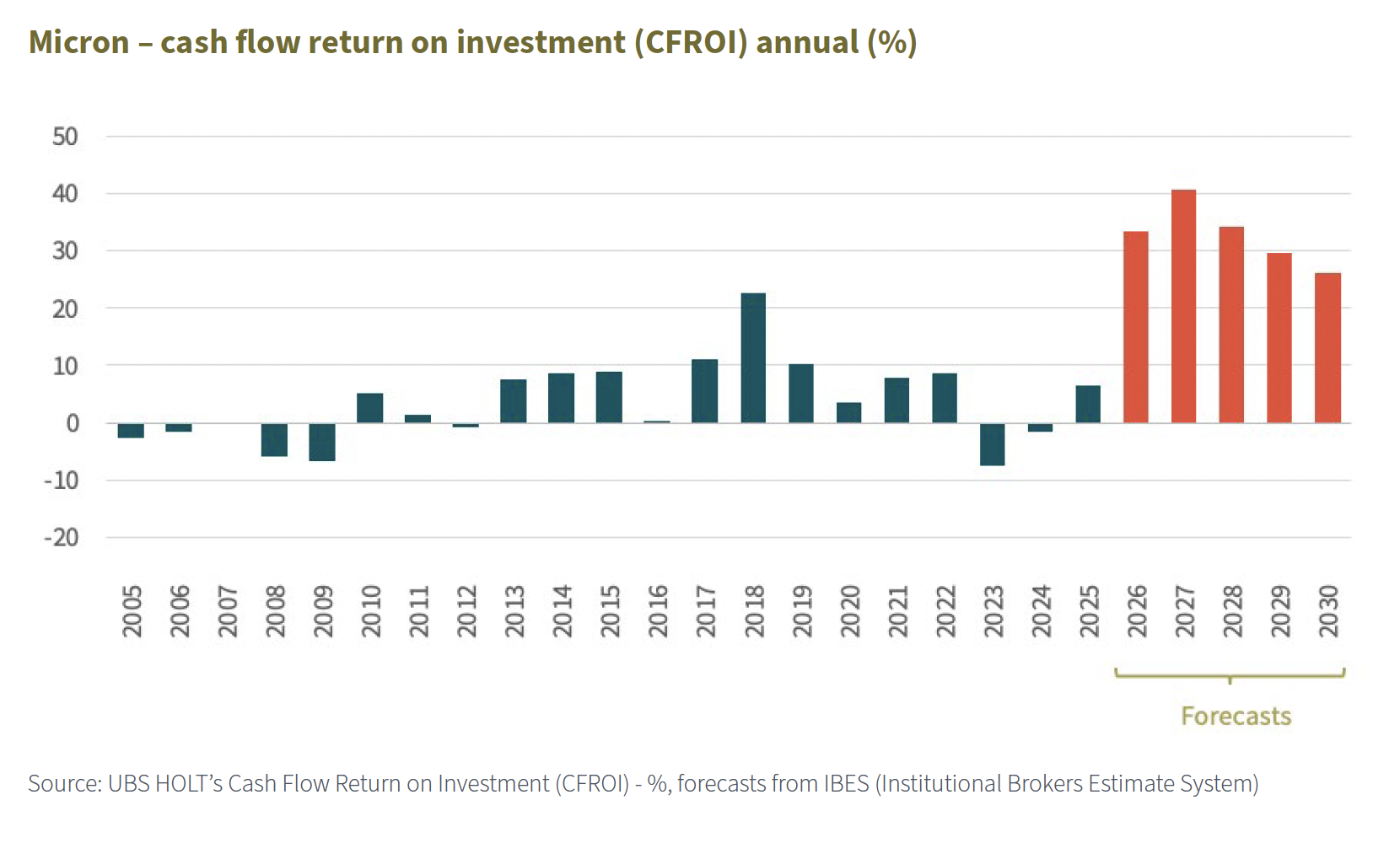
The charts below show annual Cash Flow Return on Investment (CFROI) for the past two decades for each company. SK Hynix has suffered several years of negative returns, with just three years where returns exceeded 10%. Samsung – which uses DRAM production in the manufacture of phones, laptops, TVs and other consumer products – has fared somewhat better. Like SK Hynix, Micron has delivered poor CFROI metrics.
But take a look at forecasts (in orange) for the next five years. Something appears to have changed.
A closer look at DRAM
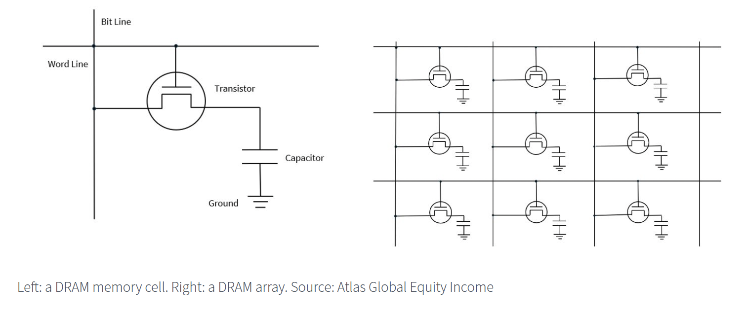
Before we dive into High Bandwidth Memory, it is useful to cover some basics. A DRAM memory cell is made up of one transistor and one capacitor and is sometimes referred to as 1T1C memory.
The image on the left above shows this configuration. When a voltage is applied to the word line – the horizontal wire – the gate of the transistor switches on. If a voltage is then applied to the bit line – the vertical wire – charge will flow through the transistor to the capacitor, loading the capacitor with charge. If voltage is then removed the charge will remain in the capacitor. A capacitor full of charge represents a “1” in the computing world, while an empty capacitor represents a “0”.
What can make things less straightforward is that charge leaks from a capacitor. DRAM memory is designed to refresh the cells containing charge on a regular basis – hence the “dynamic” prefix.
DRAM is a two-dimensional array of transistor and capacitor cells, similar to the image on the right above but on an enormous scale.
But why is it called “random-access memory”? This refers to the ability to select any cell to read or write data to.
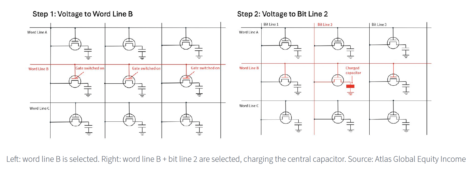
In the images above, to write data to the cell in the middle of the 3×3 array, you first select word line B, turning on all transistors in the row (see left image) and then apply a voltage to bit line 2. Charge would flow along the bit line but would only be able to enter the capacitor with the transistor gate turned on in the column, which in this example is the cell at the centre of the array.
This type of direct memory access contrasts with much older, slower types – such as magnetic tape (not to be confused with magnetic core) or drum memory – which involved scrolling through various amounts of data each time to get to the right place.
Contention
In this 3×3 array only one word line can be activated at a time. For example, if word line B and word line C are both selected then the cells in the middle column will fight to drive the same shared bit line once this is activated. This electrical conflict, called contention, corrupts the data, causes wrong reads and can create damaging current spikes.
Row decoding prevents this and ensures that only one row is selected at a time. Additionally, DRAM arrays are organised into a number of segregated banks of memory cells (typically four to 16 or more per chip) to avoid contention and allow parallel operations to take place. After all, speed is crucial.
Synchronous and double data rate
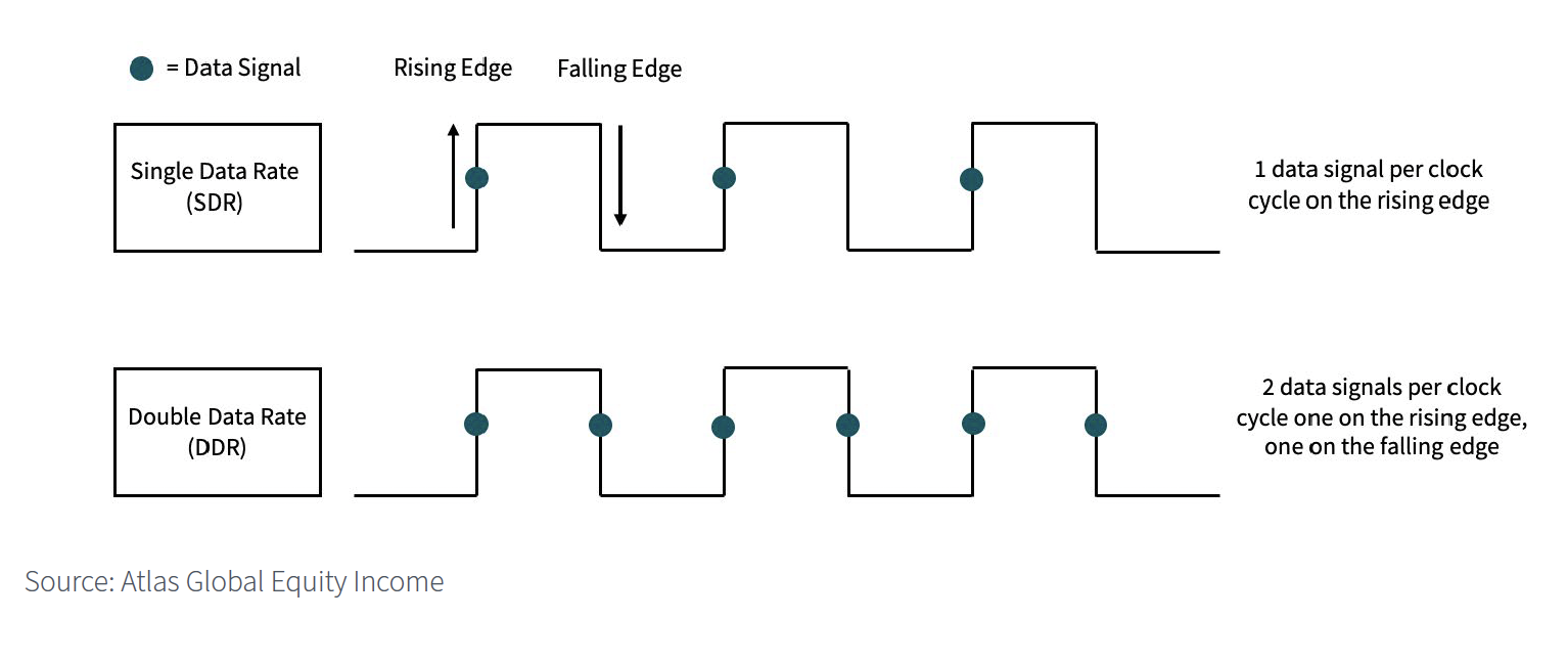
Synchronous DRAM (SDRAM) emerged in the mid-1990s. It synced memory operations to the central processing unit (CPU) clock, enabling faster and more predictable data access than asynchronous DRAM.
The advent of double data rate (DDR) in 2000 improved memory speeds further by transferring data on both rising and falling clock edges, doubling bandwidth without increasing clock speed.
![]()
As the table below shows, several generations of DDR DRAM have been released over the years. Notice how both the data rate – measured in millions of data transfers per second – and the clock speed have increased with each generation.
DDR architecture
With double data rate DRAM, the DRAM die is attached to the package substrate and packaged into a chip. The chip is then attached to the printed circuit board (PCB) of a dual In-line memory module (DIMM), also known as a memory card. The memory card has gold connectors and is slotted into the DIMM slots on the motherboard of a PC or server.
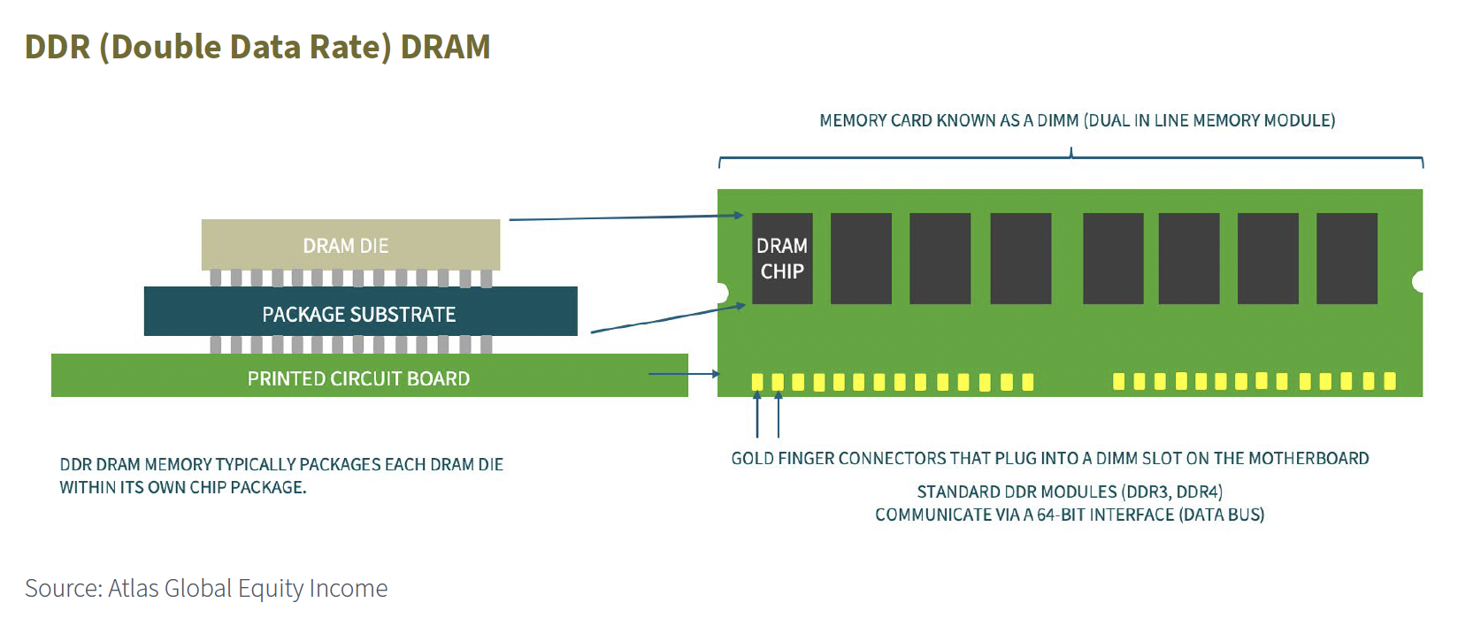
This architecture uses a standard 64-bit-wide interface (also called a bus), allowing 64 bits of data to be transferred in parallel per operation. When it is required by the GPU or CPU, data will need to make its way along centimetres of copper traces on the memory module and then on the motherboard before reaching the processing chip. In circuitry terms, the memory is a long way from where it is needed.
With each generation, the interface of 64 bits has remained broadly the same. But performance has increased by using higher clock speeds, along with other architectural improvements such as larger prefetch buffers and bank groups. These changes have significantly boosted effective bandwidth.
The memory wall
Graphics processing unit (GPU) performance began increasing rapidly in 2006-2007. It soon became clear that conventional DDR memory would struggle to supply data fast enough to keep up with GPUs. This performance challenge has become known as the “memory wall”.
Higher clock frequencies might seem like the solution. Unfortunately, this causes power consumption and heat to rise sharply. A fundamental rethink was required.
High Bandwidth Memory
Starting in 2008, AMD led the development of High Bandwidth Memory (HBM). This involved a completely different architectural approach that became known as “wide and slow” – as opposed to DDR architecture, which is often described as “narrow and fast”.
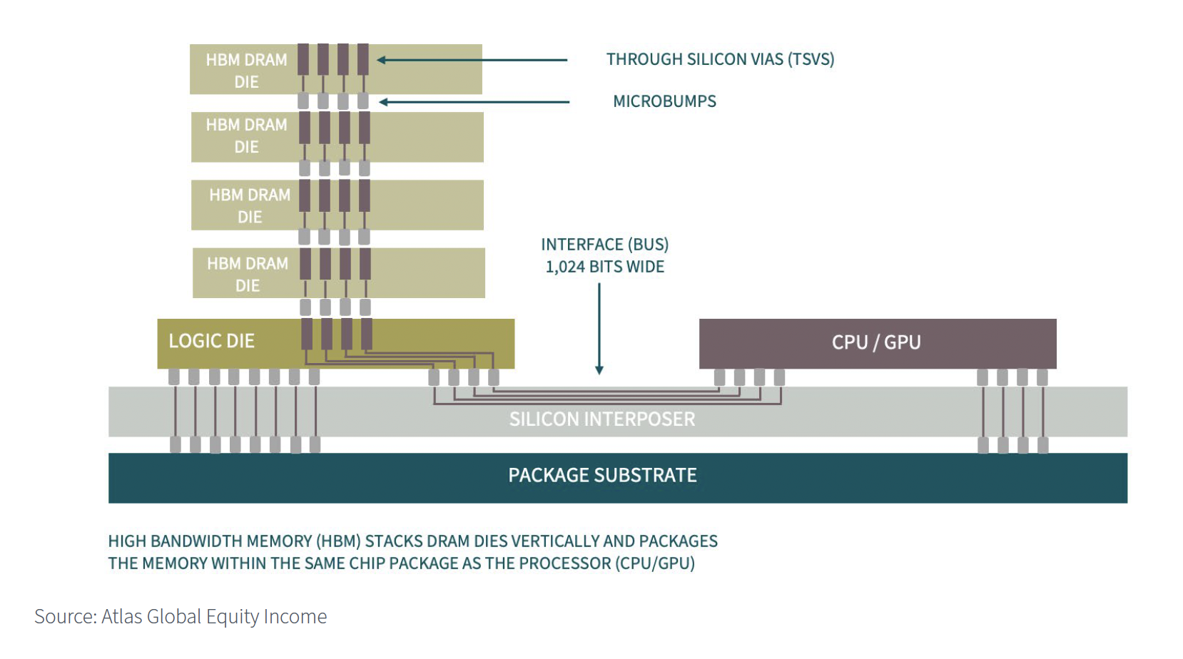
Instead of a narrow 64-bit bus (interface) running at very high speeds, HBM uses an extremely wide bus – 1,024 bits – while keeping the clock speed relatively moderate. This design delivers dramatically higher total bandwidth, with much better power efficiency and lower heat output.
Stacking multiple DRAM dies (one on top of the other) and connecting them using thousands of through-silicon vias (TSVs – tiny holes etched through the silicon and filled with copper to make the electrical connection) allows this wide 1,024-bit interface to work.
Other design features also help. Using long copper traces running across PCBs would be cumbersome and slow for such a wide interface. A DRAM stack is instead placed on what is known as a silicon interposer, which keeps the memory very close to the processor. To make the connections, the silicon is etched using photolithography. Ultra-fine copper connections are then embedded by electroplating the etched trenches. The HBM stack and processor (CPU/GPU) are then formed into a single chip package.
Remember that issue of contention? The extra DRAM dies multiply the total number of available memory banks (often 64+ across a stack), allowing the memory controller to schedule parallel data accesses without bank conflicts or row clashes.
In addition, HBM has a special logic die at the bottom of the stack which manages key tasks such as high-speed communication with the GPU, data organisation, error correction and overall control. This functionality, which used to be buried within the DRAM dies themselves, enables the HBM DRAM dies to be simplified and the logic removed to a single chip.
In order to make this design a reality, AMD partnered with SK Hynix, which produced the first HBM chip in 2013. AMD debuted the technology in the Radeon R9 Fury GPUs in 2015.
The current generation, HBM3E, delivers dramatically higher bandwidth than the present generation of “narrow and fast” architecture, DDR5. A single HBM3E stack achieves 1.15-1.22 terabits per second (Tb/s), which is roughly 15-20 times faster than a typical DDR5 DIMM. While DDR5 offers better capacity and cost for general computing, HBM3E excels in high-bandwidth
AI and GPU applications.
Price increases
Surging AI demand has driven HBM3 and HBM3E prices sharply upward, enticing the DRAM oligopoly of SK Hynix, Samsung and Micron to shift production capacity away from DDR and towards more profitable HBM. This reallocation has reduced DDR supply, pushing DDR memory prices higher as well.
Market structure
Price booms are not new to this cyclical industry, but the strength of demand and a tight market oligopoly have implications. DRAM plants are not easy to switch on overnight – they take billions of dollars of investment and years of planning. Add to that three experienced market participants that understand the horrors of oversupply and prices might just stay higher for longer.
Less commoditised
In addition, manufacturing HBM is technically challenging and does not appear to have the commoditised characteristics of DRAM from a decade ago. Major issues include managing heat and warpage in ultra-thin stacked dies, creating perfect high-density TSVs, assembling the stack using tiny solder microbumps, maintaining signal integrity across thousands of vertical connections at high speeds and performing complex pre- and post-stack testing.
As evidence of these challenges, Samsung struggled significantly with HBM3 and HBM3E production. The company faced persistent low yields, thermal management issues and excessive power consumption, resulting in delayed qualification with Nvidia and lost market share to SK Hynix. These problems forced Samsung to cut production targets and slowed its ability to capitalise on the AI boom.
Contract terms
Traditionally, the DRAM market relied on short-term contracts – usually quarterly or annual spot-market deals – which caused high price volatility. In March 2026 Micron secured its first five-year strategic customer agreement with a major unnamed hyperscaler. Press speculation suggests SK Hynix and Samsung are also pursuing similar long-term contracts with hyperscaler customers to lock in AI-driven demand.
Conclusion
The DRAM memory market has been a poor industry for many decades. Historically, it showed archetypal commodity-like characteristics – caused by fierce competition – and poor pricing power. Competition has dwindled over the decades, changing the market structure to a tight oligopoly of just three: SK Hynix, Samsung and Micron.
The increasing speed of processors, particularly graphics processing units (GPUs), led to a new memory chip design known as High Bandwidth Memory (HBM). This design enables data to reach the processor much faster and with greater efficiency.
The advent of AI training and inference has led to explosive demand for HBM. SK Hynix started mass production of the next generation of HBM, HBM4, earlier this year and stated during its Q1 2026 earnings call: “Customer demand for HBM over the next three years already far exceeds our production capacity.”
The market structure, the less commoditised nature of HBM manufacturing and increasing contract terms suggest the oligopoly is able to capture far more of the value chain than the industry ever did previously. Against this backdrop, SK Hynix is the market leader, controlling approximately 55-62% of the global HBM market.
Disclaimer:
As at the end of April 2026, Atlas Global Equity Income holds a long position in SK Hynix.
This article is not to be taken as investment advice.
Michael Foster, Fund Manager and Roger Breuer, Analyst – Atlas Global Equity Income
April 2026

………………………
| AUTHORISED AND REGULATED BY THE FINANCIAL CONDUCT AUTHORITY |
| MEMBER OF THE LONDON STOCK EXCHANGE |
| NOT FOR DISTRIBUTION IN THE U.S.A. |
This factsheet has been issued by Fiske plc on the basis of publicly available information, internally developed data and other sources believed to be reliable and accurate. No representations or warranty, expressed or implied, is made nor responsibility of any kind is accepted by Fiske plc, its directors or employees either as to the accuracy or completeness of any information stated in this factsheet. Any opinions expressed (including estimates and forecasts) may be subject to change without notice. This document is not intended as an offer to buy or sell the fund nor as a personal recommendation. Fiske plc, or any of its connected or affiliated companies or their employees, may have a position or holding or other material interest in the fund concerned or in a related investment, or may have provided within the previous twelve months, significant advice or investment services in relation to the investment concerned or a related investment.
Investors must be aware of the risks associated with investment in this fund. Full details of the Atlas Global Equity Income Fund, including risk warnings, are published in the Prospectus and Key Investor Information Document (KIID). The fund may not be suitable for all investors and if you are in any doubt whether the fund is suitable for you, advice should be sought from a suitably qualified professional advisor. The value of the fund and the income derived from it can go down as well as up. Investors may not get back their initial investment. Past performance is not necessarily a guide to future performance. Estimates of future performance are based on assumptions that may not be realised. Securities denominated in foreign currencies may see their value fall as a result of exchange rate movements. Any comments contained in this factsheet are intended only for the use of the individual or entity to which it is addressed and may contain information which is confidential and may also be legally privileged. If you have received this document in error, please telephone the Compliance Department on +44 (0)20 7448 4700. Fiske plc FCA Register No: 124279