Atlas Global Equity Income – Monthly Manager Commentary
December 2025

There was no trading activity on the portfolio in December 2025. However, it is worth noting that the spin-off from Unilever’s ice-cream business, the Magnum Ice Cream Company (TMICC), became effective on December 6 – as a result of which the number of holdings in the portfolio has increased from 36 to 37.
Featured holding – Texas Instruments
This month we highlight Texas Instruments, which was added to the portfolio during the November 2025 restructuring.
Texas Instruments (TI) is in the final stages of its extended phase of high capital investment in 300mm wafer fabrication plants, also known as “fabs”. A management update in February 2025 stated that the company was nearly 70% through a six-year elevated capital expenditure (capex) cycle that, once completed, would be able to deliver “free cash flow per share growth across a range of market conditions”. Since TI’s stated objective for cash returns is to return all free cash flow to shareholders over time through a combination of dividends and stock repurchases, the end of the cycle bodes well for future returns.
Capital expenditure
The chart below shows levels of capex between 2018 and 2020, when annual capex ranged from $649 million to $1.1 billion. The elevated capex cycle began in 2021 and is expected to complete by the end of 2026. At the time of writing (end of December 2025) capex numbers for Q4 2025 are still to be reported, but FY25 capex is expected to weigh in at about $5 billion and FY26 capex is guided at between $2 billion and $5 billion. This six-year capex cycle is now approximately 83% complete.

Texas Instruments – a brief history
Founded in 1930, Geophysical Service Incorporated provided seismic exploration services for the oil industry. During World War II the company helped the war effort by manufacturing defence electronics, which it became successful at, and after expanding into semiconductors and consumer products it was eventually renamed Texas Instruments in 1951.
The company achieved a groundbreaking milestone in 1958 when engineer Jack Kilby demonstrated the first working integrated circuit, a germanium-based device that integrated multiple electronic components on to a single chip, revolutionising electronics by enabling smaller, more efficient devices.
TI continued innovating, producing the first silicon transistor in 1954 and the world’s first hand-held calculator in 1967.
In early 1970 a company named Datapoint asked both TI and Intel to produce a single-chip microprocessor. Both designs were rejected. However, while TI never commercially released its TMX 1795 8-bit chip, Intel successfully released the world’s first microprocessor, the 4004, in November 1971, followed by the 8008 in April 1972. Intel went on to dominate this field for decades.
Outshone by Intel, TI shifted away from general-purpose microprocessors in the 1970s, successfully pivoting to specialised microcontrollers like the TMS1000 series for embedded applications in appliances, calculators and industrial controls. The company also expanded further into consumer electronics through handheld calculators and entered the DRAM memory market, with production starting in 1973.
However, the 1980s and early 1990s brought intense competition from Japanese manufacturers like Hitachi, Toshiba and NEC, which dominated DRAM and consumer electronics by using aggressive pricing, thereby eroding TI’s margins. TI faced its first financial losses, with massive write-offs from the failed TI-99/4A home computer, and was forced to lay off staff. Viewed as an unfocused conglomerate, it was in need of a rethink.
Strategic pivot
By the late 1990s TI had initiated a strategic pivot to analog semiconductors. It divested its DRAM memory operations to Micron in 1998 (memory had become a highly commoditised market) and acquired Burr-Brown, a high-performance analog specialist, for $7.6 billion in 2000, significantly broadening its analog portfolio. Between 2008 and 2012 TI exited the wireless baseband business due to Qualcomm’s dominance, and in 2011 it acquired National Semiconductor for $6.5 billion – making TI the world’s largest analog chip manufacturer.
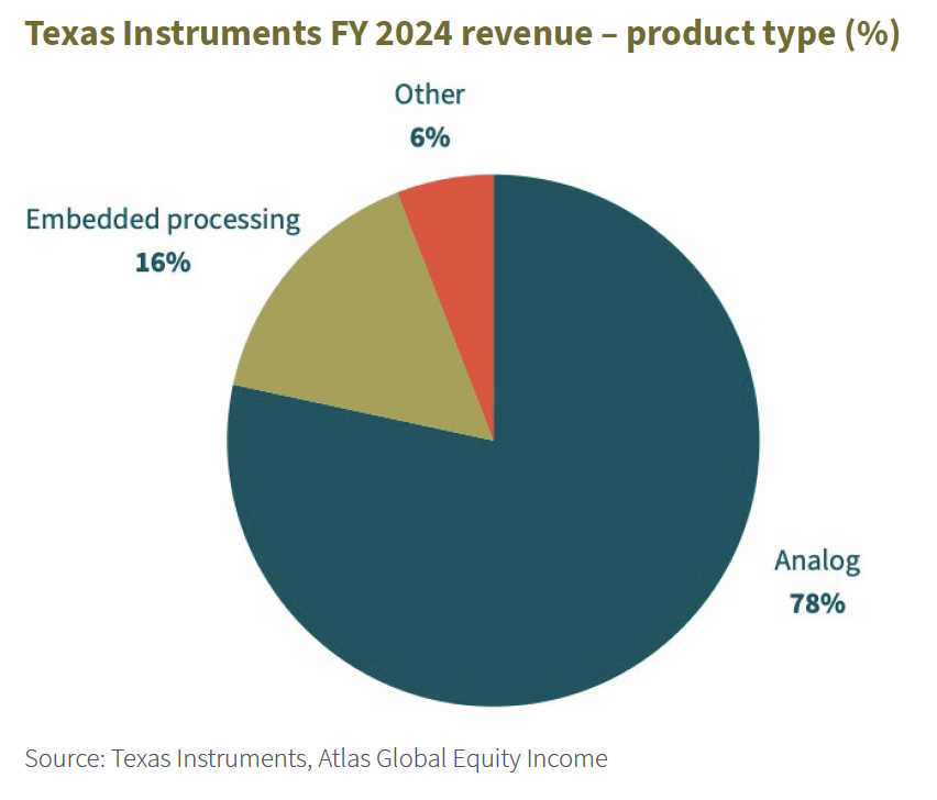
Almost 80% of TI’s revenue was derived from analog semiconductors in FY24, as shown below.
The chart below shows how TI’s strategy has successfully improved returns (as measured by Cash Flow Return On Investment – CFROI) from the mid-2000s, with returns between 2017 and 2022 consistently exceeding 30%. This is suggestive of a competitive advantage.
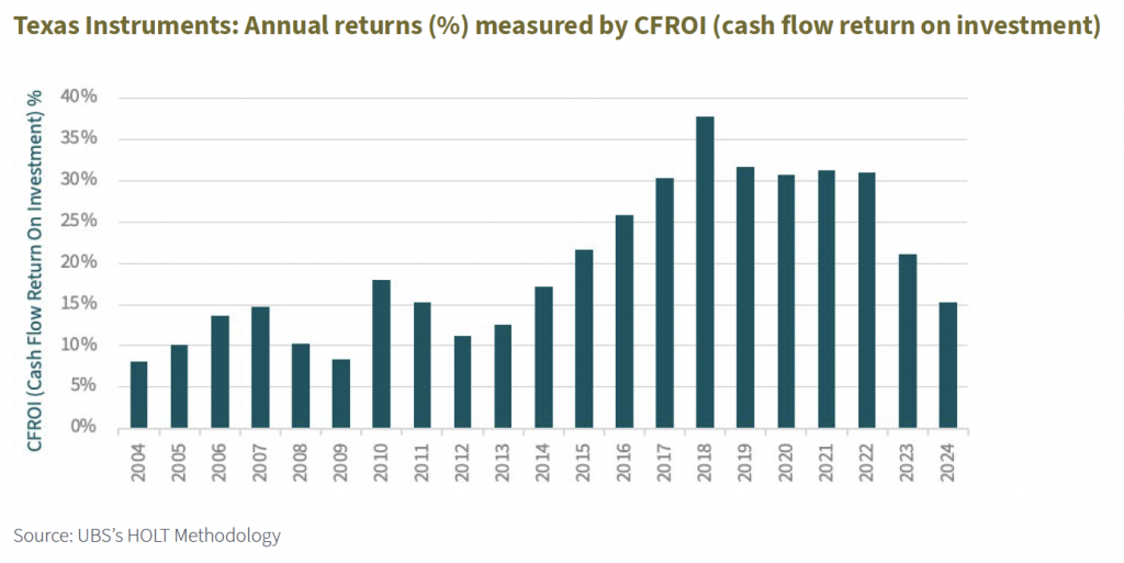
In our opinion, the decline in returns in 2023 and 2024 should be considered with reference to the recent large capex spend. Increased assets under construction that are yet to be fully productive reduce overall returns. This is about to change.
To help understand TI’s competitive advantage, it is necessary to delve a little deeper into analog semiconductors. We can start with a basic comparison of digital and analog semiconductors.
Digital versus analog
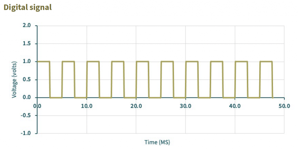
Digital signals are discrete. In other words, they represent data as distinct values, typically binary 1s and 0s, like on/off switches. Their binary nature makes them highly noise-resistant, because small distortions do not change a 1 to a 0 or vice versa. This robustness has enabled reliable long-distance transmission, error-free copying, massive scalable storage, ultra-fast processing in computers and smartphones and complex software-driven applications like machine learning. As a result, digital semiconductors, which process these signals, have dominated fields requiring raw computing power, vast data storage and high-speed digital communication.
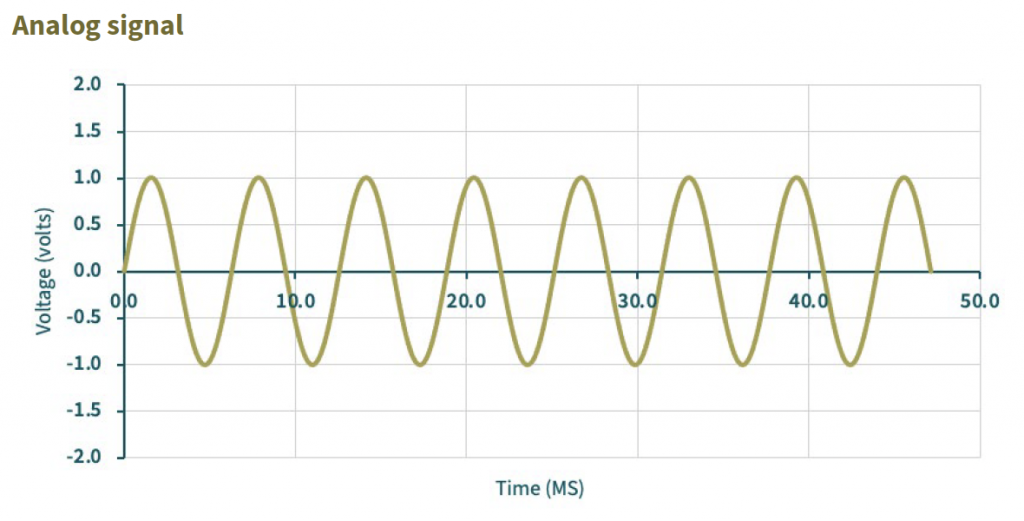
Analog signals are continuous, varying smoothly over time, much like a dimmer switch. This continuous nature makes them far better at interfacing with the real world – for example, sensing temperature, pressure, sound, light and motion. After all, the physical world is continuous, not binary. Analog signals do have a weakness: they are susceptible to noise and degradation. Analog semiconductors are designed to handle these continuous signals.
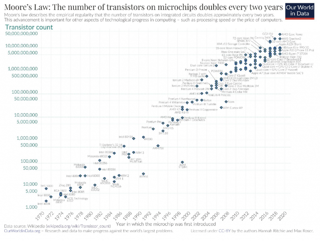
With these basic concepts covered, we can explore how digital semiconductors have resolutely followed Moore’s Law and why analog semiconductors have not.
Moore’s Law applies to digital, not analog
As you may know, Moore’s Law originated in an internal document at Fairchild Semiconductor written by Gordon Moore, a Director of R&D. In the document, entitled ‘Cramming more components onto integrated circuits’, Moore predicted that the number of components on a single silicon chip would double every 12 months.
Moore’s original 1965 prediction proved more or less accurate. A decade later, after co-founding Intel, he refined his forecast, proposing that the number of components on a silicon chip would double approximately every two years. This forecast proved even more accurate. Although we are now arguably seeing some slowdown, the maxim has proved reliable for decades.
Moore’s lesser-known prediction
Alongside what became known as Moore’s Law, Moore made a lesser-known prediction about the future of analog (or “linear”) circuits in integrated electronics. He forecast that analog circuits would not be transformed as dramatically by increasing integration density.
He wrote in his original article: “Integration will not change linear systems as radically as digital systems… The lack of large-value capacitors and inductors is the greatest fundamental limitation to integrated electronics in the linear area.”
Moore thus precisely identified why digital circuits would scale dramatically with transistor density increases while analog circuits would remain constrained by the difficulty of integrating high-quality, large-value components like capacitors and inductors on to the chip. Once again, history has proved the remarkable accuracy of this prediction.
Smaller transistors
For decades the main way to keep Moore’s Law going has been to make transistors smaller. The size of the transistor, sometimes referred to as the “process node”, originally reflected the length of the transistor’s gate and would be measured in micrometres or nanometres. A micrometre (µm, or micron) is one millionth of a metre, while a nanometre (nm) is one billionth.
Intel’s aforementioned 4004, unveiled in 1971, used 10µm (10,000nm) gates. Leading-edge process nodes are now labelled 2nm, but this designation no longer matches the actual gate length – rather, it is a term for overall density and performance gains.
Digital chips pursued size reductions aggressively for more speed and efficiency. Analog chips, however, hit serious performance problems with smaller sizes, so companies like TI still mostly produce them on mature 45nm to 130nm technology. These nodes were first commercially introduced roughly as follows: 130nm around 2001, 90nm in 2003-2004 and 45nm in 2007-2008.
The analog matching problem
For those technically minded and wanting to understand the challenges faced by smaller process nodes for analog, consider the following.
Analog circuits often rely on paired transistors that need to behave almost exactly the same. A classic example is an op amp (operational amplifier), which is one of the most common building blocks in analog electronics. The input stage of an op amp uses two matched transistors, called a differential pair, to compare two input voltages. The difference between the input voltages is then amplified and sent to the output. If there are tiny differences in the manufacture of the paired transistors – that is, if they do not match exactly – their electrical properties will differ, causing errors. The smaller the process node, the harder it becomes to make these transistor pairs identical.
The following circuit diagram, taken from a document on TI’s website, shows the transistor pairs. We have outlined them in red.
![]()
Note the text above: “Symmetry of the input stage is key to its operation.” Keeping transistors identical as process nodes shrink is just one of many challenges faced by analog semiconductors, and it is why it is important to keep in mind that the analog semiconductor market is quite different from the digital semiconductor market.
Wafer size
Another key factor to understand is the wafer size used in chip fabrication plants. For silicon chips, ingots of high-purity silicon are grown using the Czochralski process, where a seed crystal is dipped into molten silicon and slowly pulled upward while rotating to form a large cylindrical crystal ingot. This ingot is then ground to a precise diameter, sliced into thin disks using diamond wire saws and polished to create flat, defect-free, ready-to-use wafers.
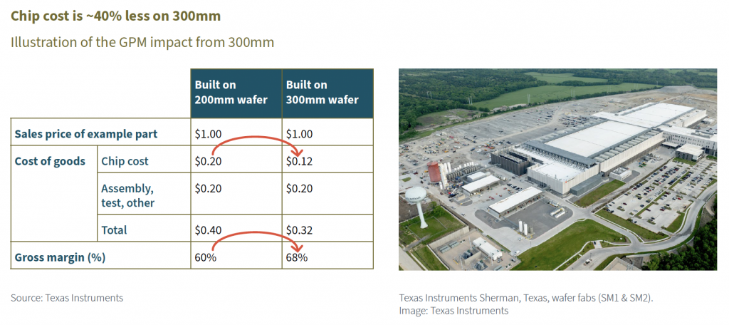
Wafer diameters have increased over the decades, from early small sizes (e.g. 50mm-150mm) to the current standards of 200mm and 300mm. 300mm wafers offer around 2.25 times more surface area than their 200mm counterparts and can accommodate significantly more dies (tiny, individual integrated circuits) per wafer, reducing per-chip costs by around 30-40% in high-volume production simply through economies of scale.
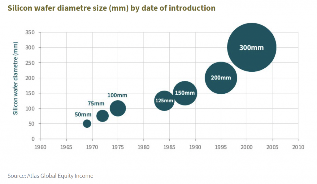
Digital semiconductors like logic chips (CPUs, GPUs, SoCs), NAND flash and DRAM transitioned swiftly to 300mm wafers, starting in the early 2000s. This shift was driven by massive production volumes and rapid payback on the enormous capital investment required for 300mm fabs (often exceeding $20 billion). Larger wafers work well with cutting-edge lithography tools like Extreme Ultra Violet (EUV) and full automation systems, making 300mm digital semiconductors a success.
In contrast, analog semiconductors like power management integrated circuits, amplifiers, sensors, radio frequency devices and micro-electromechanical systems have largely remained on 200mm wafers. The economics simply did not make sense when 300m wafers were first introduced, as analog semiconductors were characterised by lower production volumes. Additionally, they typically involved longer product lifecycles, often 10-15 years for automotive/industrial applications. Since products used in automotives, for example, undergo a process of pre-qualification before being designed into a vehicle, a change of manufacturing would trigger re-qualification. For these reasons and others, analog prioritised reliability and precision and initially stayed with the better-known 200mm wafer technology, avoiding the economic and technical challenges of the upgrade.
One key technical challenge of moving from 200mm to 300mm wafers was achieving uniform temperature distribution across the larger wafer surface during processes like rapid thermal processing, annealing and deposition. The increased diameter (2.25x greater area) leads to greater thermal mass, longer ramp-up times (approximately 1.7x longer to reach target temperatures) and higher risk of temperature gradients across the wafer. In turn, this could lead to defects and inconsistencies. In analog circuitry, as we have discussed, transistor pairs must exhibit near-perfect matching. Any significant mismatch renders them unsuitable. Initially, 300mm wafers were simply too big a risk to take.
TI’s 300mm opportunity
TI had watched the introduction of 300mm wafers from the sidelines through much of the early 2000s, as the expensive transition was spearheaded by high-volume DRAM and logic manufacturers. By 2007 the company had constructed the shell for its Richardson Fabrication (RFAB) facility in Richardson, Texas, originally planning a 200mm analog fab. A pivotal opportunity presented itself in 2009 with the bankruptcy of Qimonda, a major DRAM producer crippled by the global financial crisis and a severe drop in memory prices. TI acted and acquired a vast array of advanced 300mm production equipment from Qimonda’s fab in Richmond, Virginia. The plant was originally part of a facility built and equipped at a cost of approximately $3 billion. TI picked up the equipment at a deeply discounted $172.5 million, effectively securing an entire modern toolset at a fraction of new equipment costs. The economic risks of 300mm for analog were worth taking at this price. In addition, many of the 300mm technical issues were being overcome by then in any event.
This opportunity enabled TI to develop its RFAB facility as the world’s first dedicated 300mm analog fabrication plant, unlocking 30-40% cost reductions per die for high-volume analog and mixed-signal products while maintaining the precision required for the business’s market-leading portfolio. The Qimonda acquisition not only accelerated TI’s entry into 300mm manufacturing but also established a lasting competitive edge, paving the way for subsequent expansions and solidifying the company’s dominance in analog semiconductors.
TI’s 300mm transition
Today, with demand for analog chips in automotive and industrial sectors growing and with many of the technical challenges of 300mm now overcome, TI has embarked on a strategy of building out this 300mm capability.
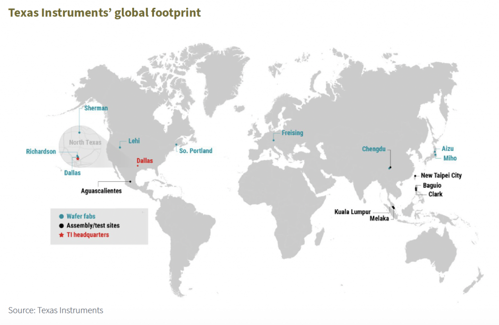
The focus of this investment is North America. Specifically, TI’s 300mm wafer plans are primarily focused on three locations: Richardson, Lehi and Sherman.
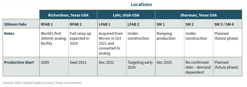
First production at SM1
In December 2025 TI announced first production at its SM1 fab in Sherman, Texas.
The company’s 300mm strategy is being realised and, crucially, is providing a path to significantly cheaper products.
Conclusion
Texas Instruments has built a formidable skill set in analog semiconductors since pivoting in the late 1990s. Its business exhibits economic returns indicative of a competitive advantage.
We have used this commentary to try to explain some of the differences between analog and digital semiconductors and the nuances of the industry.
Gordon Moore correctly forecast how analog would not scale like digital. More recently, Bob Dobkins, founder of Linear Technologies (now part of Analog Devices), has described how analog design requires a deep understanding of how components interact and influence each other – unlike digital design, where signals are idealised. Dobkins wrote a book, ‘Analog Circuit Design, Volume 2: Immersion in the Black Art of Analog Design’, emphasising the need for experience and even suggesting: “Good analog engineers are in demand and will always have a job.”
Analog design is a skill set that takes years to develop and is difficult to replicate. We would argue that this enables high returns to endure over long periods.
As discussed, TI is in the final year of a six-year extended capex cycle, investing in 300mm wafer fabrication plants in North America. These facilities offer the ability to produce chips 40% cheaper than 200mm wafer production. In our opinion, this price advantage will reinforce TI’s market-leading position and help the company to defend its competitive advantage.
Michael Foster, Fund Manager and Roger Breuer, Analyst – Atlas Global Equity Income
December 2025

………………………
| AUTHORISED AND REGULATED BY THE FINANCIAL CONDUCT AUTHORITY |
| MEMBER OF THE LONDON STOCK EXCHANGE |
| NOT FOR DISTRIBUTION IN THE U.S.A. |
This factsheet has been issued by Fiske plc on the basis of publicly available information, internally developed data and other sources believed to be reliable and accurate. No representations or warranty, expressed or implied, is made nor responsibility of any kind is accepted by Fiske plc, its directors or employees either as to the accuracy or completeness of any information stated in this factsheet. Any opinions expressed (including estimates and forecasts) may be subject to change without notice. This document is not intended as an offer to buy or sell the fund nor as a personal recommendation. Fiske plc, or any of its connected or affiliated companies or their employees, may have a position or holding or other material interest in the fund concerned or in a related investment, or may have provided within the previous twelve months, significant advice or investment services in relation to the investment concerned or a related investment.
Investors must be aware of the risks associated with investment in this fund. Full details of the Atlas Global Equity Income Fund, including risk warnings, are published in the Prospectus and Key Investor Information Document (KIID). The fund may not be suitable for all investors and if you are in any doubt whether the fund is suitable for you, advice should be sought from a suitably qualified professional advisor. The value of the fund and the income derived from it can go down as well as up. Investors may not get back their initial investment. Past performance is not necessarily a guide to future performance. Estimates of future performance are based on assumptions that may not be realised. Securities denominated in foreign currencies may see their value fall as a result of exchange rate movements. Any comments contained in this factsheet are intended only for the use of the individual or entity to which it is addressed and may contain information which is confidential and may also be legally privileged. If you have received this document in error, please telephone the Compliance Department on +44 (0)20 7448 4700. Fiske plc FCA Register No: 124279