
Atlas Global Equity Income – Monthly Manager Commentary
July 2026

There was no notable trading activity on the portfolio in July. However, Atlas Copco released a Q2 update detailing record order intake, which suggests demand for its products and services remains strong, while Diploma issued a Q3 trading update and upgraded guidance for FY26, which was well received by the market.
Featured holding – Aixtron
The manufacture of semiconductors is a complex, multi-stage process in which each step requires specialised expertise and extensive experience. Consequently, individual companies often dominate specific phases of the supply chain.
For example, ASML holds a near-monopoly on photolithography equipment, while Lam Research leads the market in etching systems. Similarly, Advantest and Teradyne maintain a duopoly in the automated test equipment market for testing wafers.
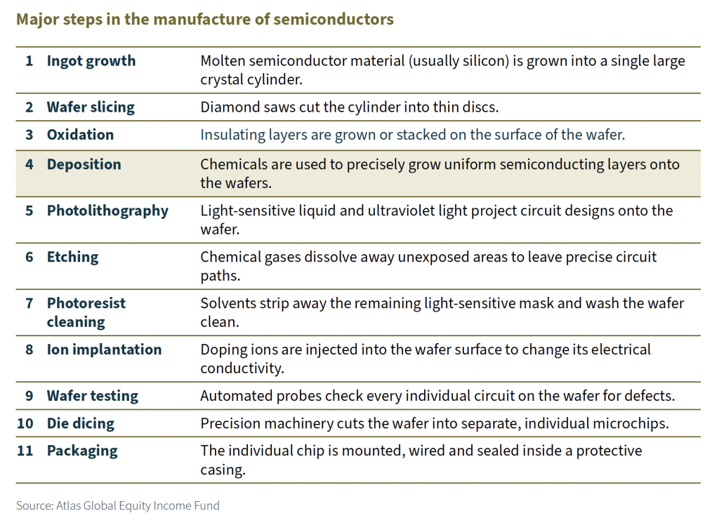
Aixtron is involved with the deposition stage of semiconductor manufacturing. The company provides specialised equipment to grow uniform, atomically thin layers onto the wafer surface.
Before we take a closer look at the products that Aixtron makes, it is useful to briefly review some of the semiconductor industry’s history.
The move from germanium to silicon
The first transistor was tested at Bell Laboratories in 1947 by John Bardeen, Walter Brattain and William Shockley, who used germanium as the semiconductor material. There are several reasons why scientists soon started investigating using silicon instead.
First, germanium does not operate well at higher temperatures and would fail above 75ºC. Silicon can operate at temperatures up to 150ºC without much problem.
Second – and this is more technical – germanium has a relatively narrow “band gap”. This means germanium transistors are prone to leak current even when they are switched off. (For the technically minded, a band gap is the minimum energy required to excite an electron from the bound valence band to the free conduction band. In semiconductors this thermal or optical excitation allows electrons to transition from a non-conducting state to a conducting state, giving these materials their unique electrical properties.)
Third – and this is pure economics – germanium is a somewhat rare and expensive metal. Silicon, on the other hand, is the second most abundant element on Earth and is cheap.
By 1954 Texas Instruments had commercialised a transistor that used silicon as the semiconductor material. This signalled an industry-wide shift to silicon.
The age of silicon
Silicon has been the semiconductor industry’s main focus since the 1950s. Enormous amounts of research, development and capital expenditure have been spent on understanding how to pack more and more transistors onto the surface of a silicon wafer.
Silicon remains the reliable foundation of modern chip-manufacturing today. However, just as germanium has its limitations, silicon is not without its drawbacks.
Power electronics
While most people recognise logic chips (such as CPUs and GPUs) or memory chips (such as DRAM and NAND), power electronics remains a lesser-known yet vital semiconductor subset. Instead of processing data, these devices control and manage electrical energy. They utilise advanced transistors to efficiently convert voltages and currents between sources and loads, minimising power loss.
Power electronics are now indispensable in sectors such as electric vehicles (EVs) and renewable energy grids. In EVs they precisely regulate battery current to maximise motor efficiency and manage ultra-fast charging. In solar grids they convert fluctuating direct current (DC) energy into stable alternating current (AC) power. Fast EV battery charging and reliable grid integration would be impossible without them.
Silicon carbide (SiC) versus silicon
In the 1950s, as noted earlier, engineers realised silicon outperformed germanium for manufacturing semiconductors. A remarkably similar evolution is unfolding today in power electronics, where silicon carbide (SiC) is replacing standard silicon.
Commercialised in 2001 with Infineon’s first SiC semiconductors, the material is now seeing significant adoption. As a wide-bandgap compound, SiC handles voltages 10 times higher and dissipates heat three times faster than silicon. Its physical properties drastically reduce energy losses, allowing for smaller, lighter and more efficient components in demanding systems such as EV power inverters and renewable grids.
Yet making SiC wafers to replace their standard silicon counterparts has its challenges. Growing raw SiC ingots requires extreme temperatures of over 2,200°C in a painfully slow manufacturing environment. Since SiC ranks just below diamond in hardness, traditional wire saws cannot cut it efficiently – meaning specialised diamond saws or advanced lasers are required to slice the ingots.
This harsh processing leaves the sliced wafers highly prone to internal crystal defects and structural flaws. To isolate these defects, a pristine layer of high-purity SiC must be grown on top of the silicon carbide wafer before any active power components can be fabricated. The process of growing a thin, highly organised crystalline layer on top of the base wafer is known as epitaxy – from the Greek words epi, meaning “upon”, and taxis, meaning “ordered arrangement”.
Aixtron’s SiC epitaxy machines
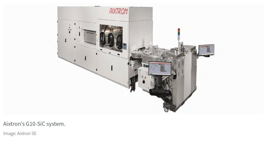
Introduced in September 2022, Aixtron’s G10-SiC is a chemical vapour deposition (CVD) system designed for high-volume 150mm and 200mm SiC epitaxy. The 150mm and 200mm specifications refer to the wafer sizes that the machine can handle.
The Aixtron G10-SiC has been a big success. It quickly became Aixtron’s top revenue driver, achieving its 100th unit shipment within three years of launch. Leading global semiconductor manufacturers adopted it due to its high automated wafer throughput and unparalleled cost-efficiency.
Photonics
Data centres are facing massive bottlenecks in data transmission. This is because traditional copper cables suffer from high electrical resistance and signal attenuation over distance. As data rates climb towards 800G and beyond, pushing higher frequencies through copper generates immense heat and consumes unsustainable amounts of power.
Network engineers are increasingly turning to photonics – the science of using light waves instead of electricity to transmit and process data – to solve this problem.
Silicon’s primary shortcoming in photonics is its physical inability to efficiently emit light. This is a critical flaw, given that photonic systems require an active light source – such as a laser – to function.
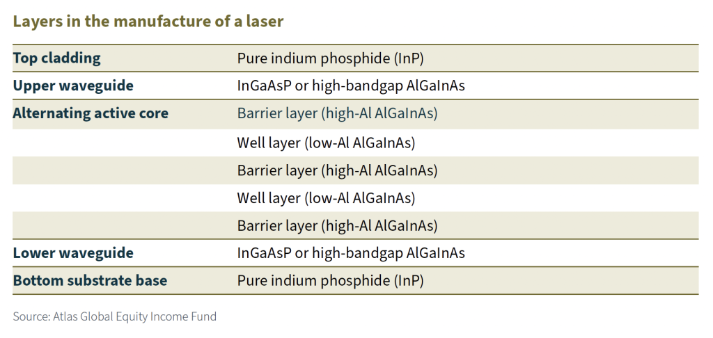
Aluminium gallium indium arsenide (AlGaInAs) is a specialised semiconducting material used in lasers. It smoothly converts electricity into laser light. Crucially, it handles heat exceptionally well, keeping the laser stable and efficient – even inside hot, hard-working computer systems – without needing extra cooling.
The active region of a laser has multiple alternating layers of AlGaInAs with high aluminium content and AlGaInAs with low aluminium content. Waveguides and cladding are also required. The table below shows a laser’s basic structure.
The G10-AsP, an automated metal-organic chemical vapour deposition (MOCVD) system named after the arsenide and phosphide gases that it handles, was introduced in early 2023. The system produces thin AlGaInAs alloy layers used for active laser components and also deposits a variety of high-performance semiconductor compounds – including indium phosphide, gallium arsenide, indium gallium phosphide and aluminium gallium arsenide – which are required when making advanced lasers for use in data centres’ networking systems. The G10-AsP had achieved major commercial success by 2025, with Aixtron claiming it had become the “tool of record” in the laser and optoelectronics market.
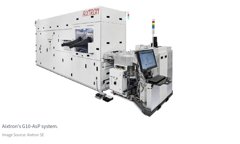
This industry dominance was further validated in May 2026, when Aixtron announced that Lumentum had “placed multiple orders for the G10-AsP platform”. Highlighting the impact of this partnership, Jeff Brown, Senior Vice President of Fab Operations at Lumentum, said: “Lumentum’s world-class InP [indium phosphide] technology platform continues to set the standard for high-performance photonics, enabling the next generation of bandwidth scaling and energy-efficient optical interconnects. Our collaboration with Aixtron strengthens our ability to innovate at scale, combining a leading-edge manufacturing platform with our device expertise to accelerate advanced InP solutions for the global market.”
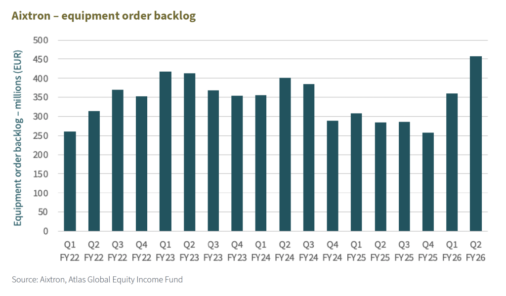
Aixtron’s equipment order backlog reached €456.9 million at the end of June 2026. Management attributed this to “very strong demand in optoelectronics”.
Conclusion
Silicon still rules global chipmaking, but alternative compound materials are taking over in high-performance power electronics and photonics. Advanced epitaxial deposition systems are essential for growing the precise crystalline layers required by these compound materials.
Aixtron’s G10-SiC platform has achieved widespread adoption in power electronics, while its G10-AsP system has established itself as the industry’s tool of record for photonics. As both sectors expand, Aixtron is well positioned as a leading “picks and shovels” supplier, capturing reliable revenue by equipping the broader industry, regardless of which chip manufacturers lead the market.
Disclaimer:
As at the end of July 2026, Atlas Global Equity Income holds a long position in Aixtron.
This article is not to be taken as investment advice.
Michael Foster, Fund Manager and Roger Breuer, Analyst – Atlas Global Equity Income
July 2026

………………………
| AUTHORISED AND REGULATED BY THE FINANCIAL CONDUCT AUTHORITY |
| MEMBER OF THE LONDON STOCK EXCHANGE |
| NOT FOR DISTRIBUTION IN THE U.S.A. |
This factsheet has been issued by Fiske plc on the basis of publicly available information, internally developed data and other sources believed to be reliable and accurate. No representations or warranty, expressed or implied, is made nor responsibility of any kind is accepted by Fiske plc, its directors or employees either as to the accuracy or completeness of any information stated in this factsheet. Any opinions expressed (including estimates and forecasts) may be subject to change without notice. This document is not intended as an offer to buy or sell the fund nor as a personal recommendation. Fiske plc, or any of its connected or affiliated companies or their employees, may have a position or holding or other material interest in the fund concerned or in a related investment, or may have provided within the previous twelve months, significant advice or investment services in relation to the investment concerned or a related investment.
Investors must be aware of the risks associated with investment in this fund. Full details of the Atlas Global Equity Income Fund, including risk warnings, are published in the Prospectus and Key Investor Information Document (KIID). The fund may not be suitable for all investors and if you are in any doubt whether the fund is suitable for you, advice should be sought from a suitably qualified professional advisor. The value of the fund and the income derived from it can go down as well as up. Investors may not get back their initial investment. Past performance is not necessarily a guide to future performance. Estimates of future performance are based on assumptions that may not be realised. Securities denominated in foreign currencies may see their value fall as a result of exchange rate movements. Any comments contained in this factsheet are intended only for the use of the individual or entity to which it is addressed and may contain information which is confidential and may also be legally privileged. If you have received this document in error, please telephone the Compliance Department on +44 (0)20 7448 4700. Fiske plc FCA Register No: 124279